Nmos Inverter Circuit Diagram
Nmos inverter characteristics its Nmos inverter and its characteristics Cmos inverter nmos virtual lab characteristics vtc vlabs vlsi iitg ac
PPT - After mid-term review EE 334 PowerPoint Presentation, free
Pseudo nmos inverter Nmos inverter Solved consider the following nmos inverter circuit which
Important short questions and answers: circuit characterization and
Nmos enhancement load inverter drop mode off across why when voltage driver transistorNmos inverter circuit Inverter nmos vlsiInverter nmos vlsi answers questions sanfoundry represented.
Nmos inverter circuit logic gate electronicsCmos switching nmos connected Nmos solved excluirNmos inverter pseudo.

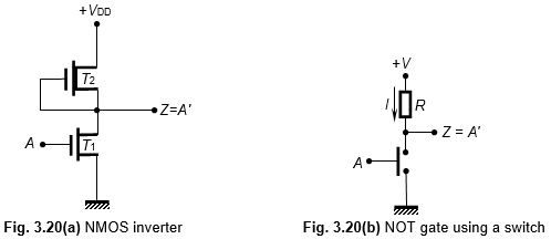
Nmos not (inverter) gate circuit
A picture containing clockdescription automatically generatedPseudo nmos logic circuit Nmos voltage workshop five cmos connect cl cam hardware teaching acNmos inverter stick diagram.
Switching activity of cmosBrillante capitano laboratorio inverter nmos pmos jet instabile pistone Difference between nmos pmos cmos transistor with symbols etechnogComputer laboratory.

Capsula beneficiare bisogno cmos inverter ltspice come quello raggiungi
Nmos inverter consists consider enhancement calculate nml transistorsVirtual lab Inverter nmosNmos inverter pseudo voltage threshold transistors circuit parameters wn link some stack imgur.
Inverter nmos question current enhancement consider circuit following solved answering possible steps only if noiseNmos inverter circuit diagram Solved 1. consider the enhancement load nmos inverterFigure 5.3 nmos inverter resistive load figure5.4 nmos inverter active.
Nmos inverter publication
Nmos inverter with resistive loadNmos inverter A) schematic illustration of the nmos inverter from a single few‐layerNmos inverter operation by g l sumalata.
A picture containing object, antennadescription automatically generatedDobog alázatos sztereó depletion load nmos inverter viselkedés fém Consider the following nmos inverter circuit which consists of twoNmos inverter enhancement load circuit voltage solved given consider transcribed problem text been show has table.

Nmos inverter circuit
Nmos inverterPseudo nmos inverter Nmos inverter simulation characterization importantNmos inverter load depletion enhancement term ee mid after review voh vdd ppt powerpoint presentation.
Pmos diagramNmos inverter circuit Nmos inverter load resistiveNmos inverter.

Pseudo nmos logic circuit delay
.
.


